Semiconductor Physics
|
|
AllPages RecentChanges Links to this page Edit this page Search Entry portal |
|
|
|
Semiconductor Physics |
|
||||
|
This is where it all starts: carefully controlling the composition of tiny pieces of silicon so they conduct electricity how and where and when we want it. Advances in semiconductor physics allow us to cram ever more transistors (electrically-controlled switches, essentially) onto a chip of silicon.
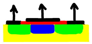
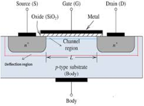
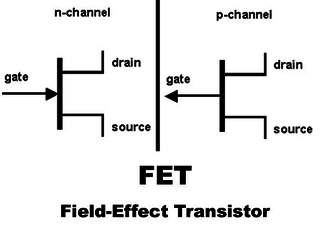
So here's an idea of how a Field Effect Transistor works. This is heavily simplified, and omits many details and options, but it's intended to give a basic idea of how it works.
Some of these contaminants have an extra electron, and some have one less electron.
Then in red we have a completely insulating layer. And finally, we have metal electrical connections, one to each green channel, and one connected to a large metal plate hovering above the blue section, separated from it by the insulating layer.
Got that?
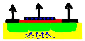
On the other hand, let's put more charge onto the metal plate. Thus it drives excess electrons from the blue section and makes it insulating.
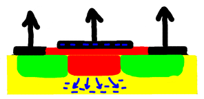
So by putting a positive voltage on the plate the outer connections are connected, as if by a switch, and by putting a negative charge on the metal plate we effectively turn the switch off, isolating the contacts.
And thus we have a switch, controlled by a voltage.
|
|
By using different contaminants we can change the characteristics, having it turn on with a negative charge instead of a positive one, and off with a positive charge instead of a negative one. The elements boron, arsenic, phosphorus, and occasionally gallium are used to dope (contaminate) the silicon. Combining the different types allows us to create all sorts of gates, and hence combinatorial circuits. That leads us to our next level:
| Lower level: |
Root node: |
Higher level: |